Johnny's home-built CPU corner (and other stuff, maybe)
8080 CPU, built entirely by DTL-technology
The ALU was the first part in this project. I had some thoughts about how do to this but it was not until I came across Viktor's amazing 4-bit processor I made the decision to use a BUS instead of some MUX (Victor uses a lot of 3S-buffers and it makes things simpler). You can se his ALU here.
I have seen otherwise that a bunch of MUX:es are popular to select one ALU function. A BUS structure makes more sense, especially when I'm designing my BUS:es to use open collector. It helps reduce the complexity a lot!
However, lack of BUS-drivers will degrade performance but a simpler solution as OC makes up for it.
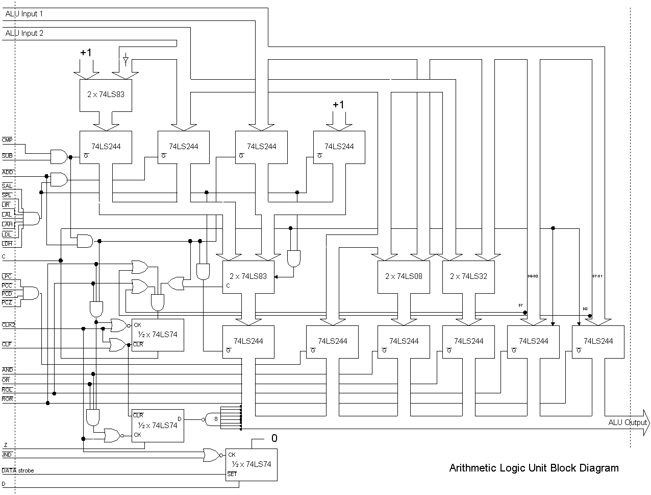
This is a overview of my ALU. Note, FLAGS are part of the ALU but is not included here.
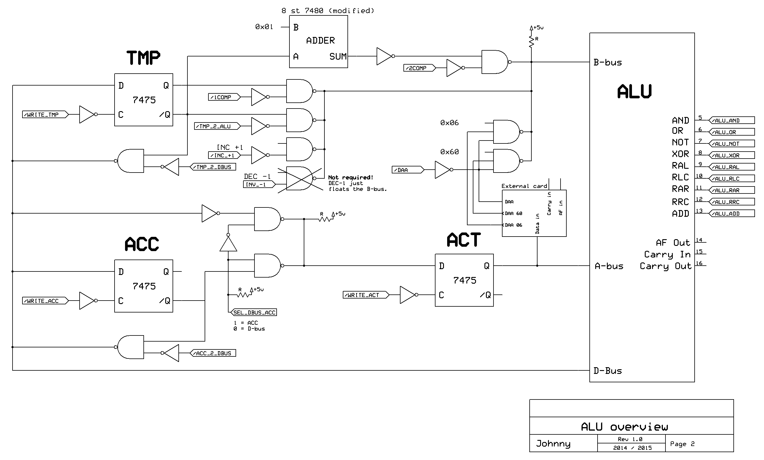
And this is how everything is connected. CARRY and other FLAGS are at the bottom.
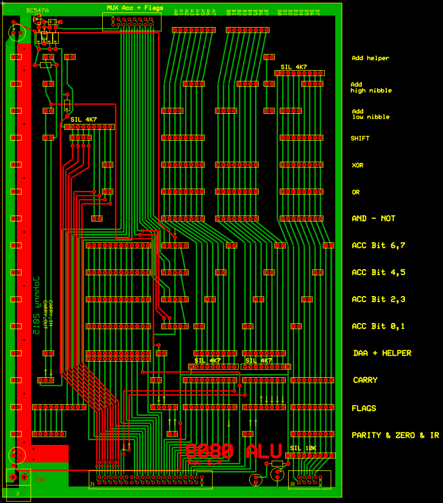
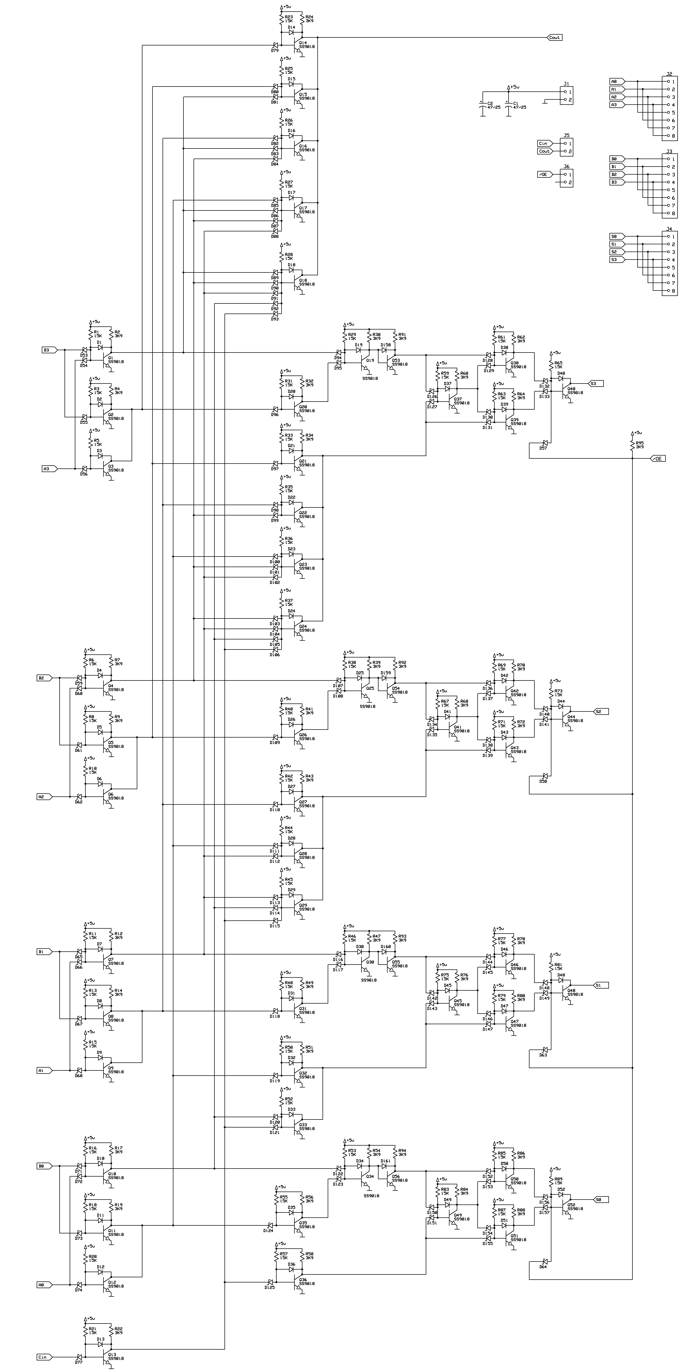
Image of the ALU, version 2.4.
Unfortunately I have a feeling that it might be time for a 2.5 version soon. Sigh...
I started by building the ALU itself and I was later going to add the ACC, ACT and TMP on a separate circuit board, and connect them by ribbon cables. It makes sense to break up complex things into smaller parts and joining them together at a later point.
So, I actually did make a ALU base board with just the ALU-stuff, but when I started trying to figure out how "the rest" should go hand in hand with the ALU I found it easy to combine both the ALU and accumulator onto one big base board.
My ALU is therefore an combination of accumulator and all there is to connect everything together.
Compare it to the picture below.
ALU Functions
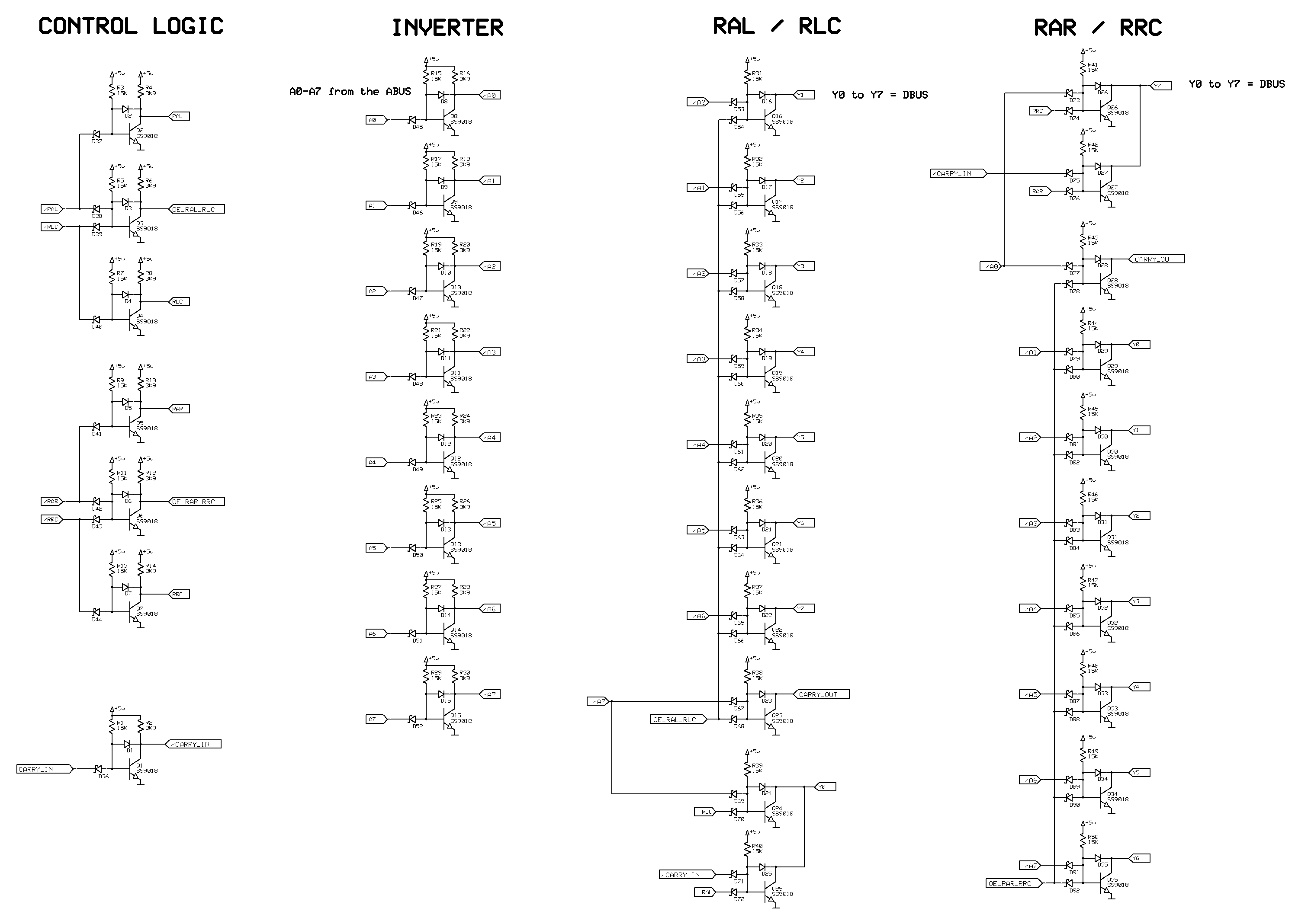
Shift functions by using some 3S buffers.
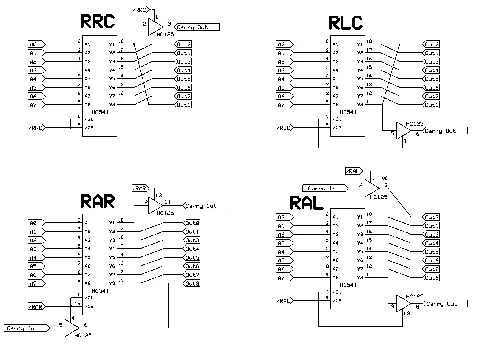
Same shift functions now implemented by transistors.
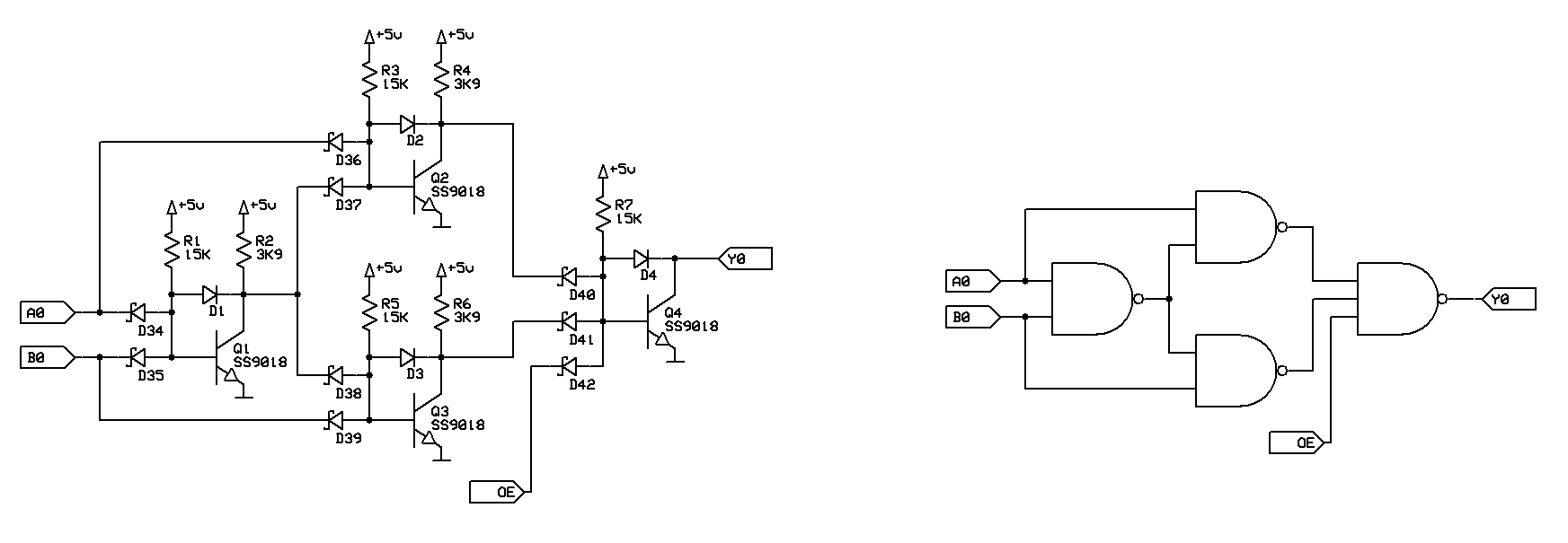
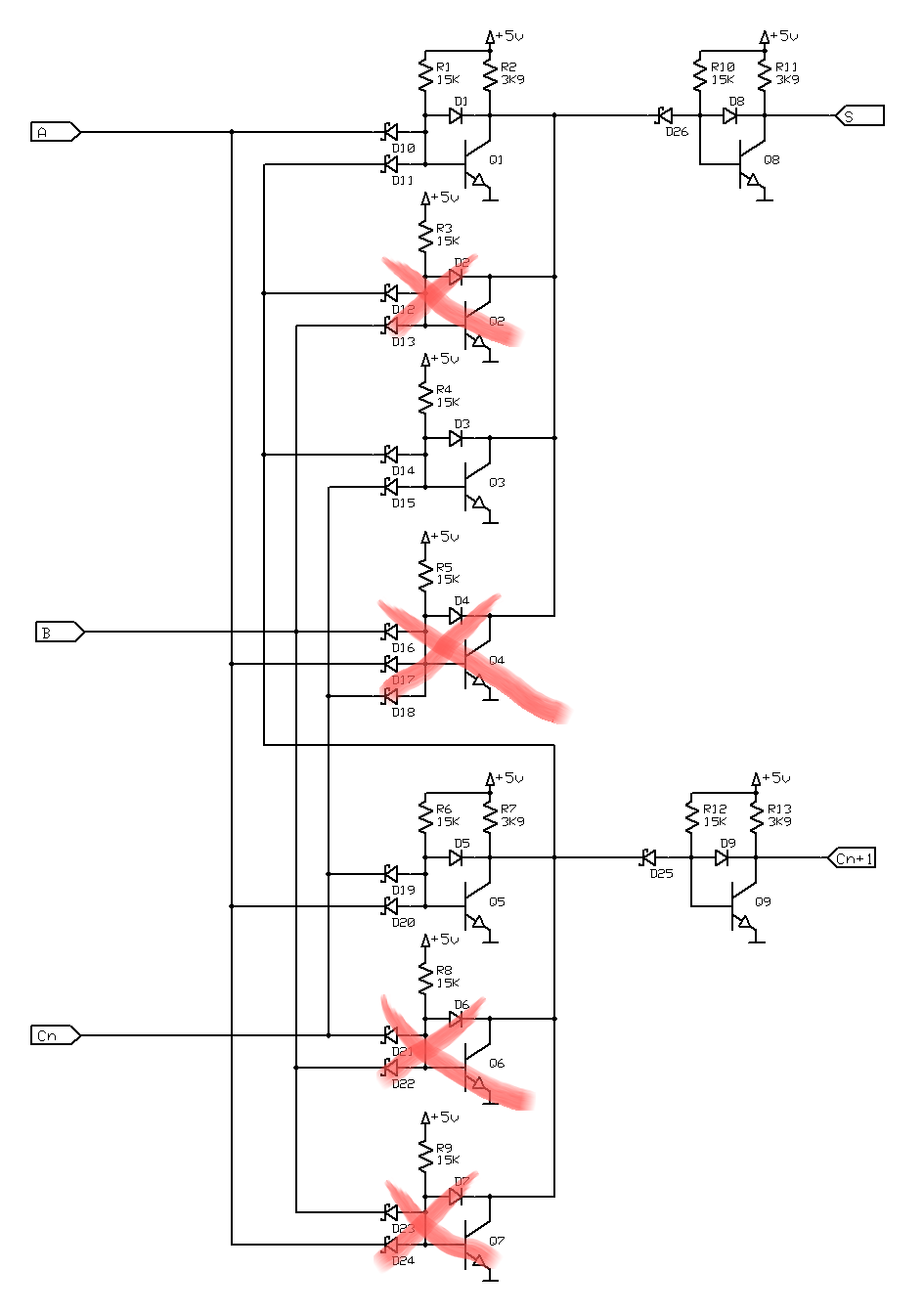
The XOR part of the ALU is fairly conventional : 4 NAND gates. By changing the last NAND to a tripple input one and the fact I'm using open collector buses makes it easy to interface the XOR. The same technique is used in my 4 bit adders.
OR function
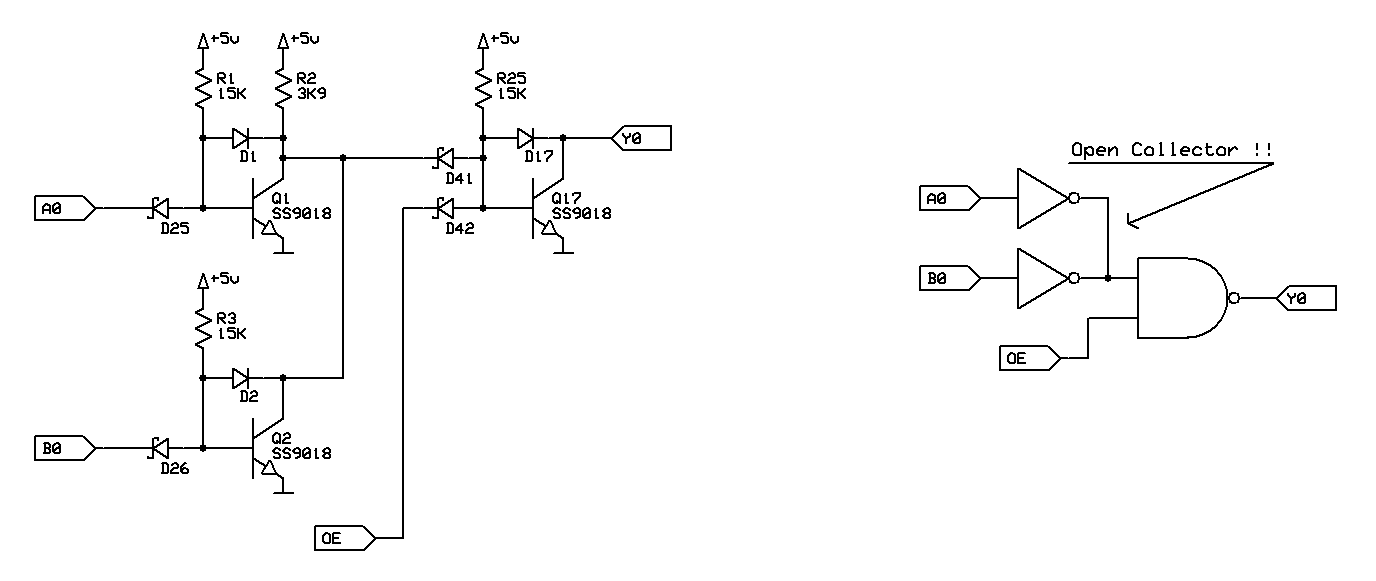
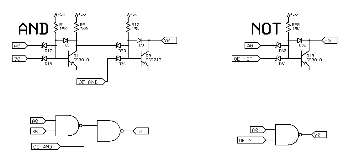
The AND and NOT function.
ADD function. Two of these is used in the ALU and four more as address incrementer/decrementer.
ALU Registers and 2-Comp Adder
Here we have the ACC, ACT and TMP registers, and also the 2-COMP Adder. The registers is simple transparent latches.
The 2-comp adder is a reduced 7480 full adder; The complemented value is taken from the TMP /Q-output and adding one is accomplished by the use of CARRY. Using the adders A-input and Carry leaves the B-input to be tied to a low (zero) value. If you study the full schematic of the 7480 you can see that some transistors never comes into play, and therefore they can be removed from the circuit.

7480 full adder

Unnecessary transistors in a reduced 7480
DAA logic.


More to follow - later.
Homebuilt CPUs WebRing
Join the ring?
To join the Homebuilt CPUs ring, drop Warren a line, mentioning your page's URL. He'll then add it to the list.
You will need to copy this code fragment into your page (or reference it.)
Note: The ring is chartered for projects that include a home-built CPU. It can emulate a commercial part, that′s OK.
But actually using that commercial CPU doesn′t rate. Likewise, the project must have been at least partially built: pure paper designs don′t rate either.
It can be built using any technology you like, from relays to FPGAs.