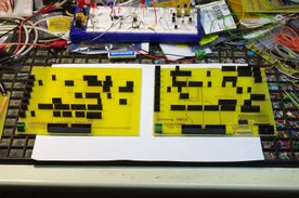
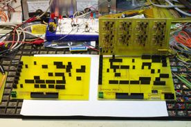
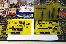
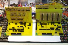
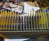
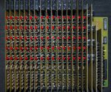
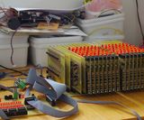
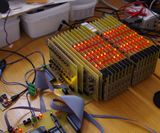
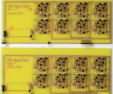
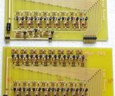
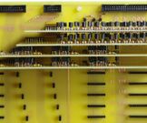
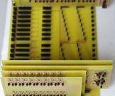
Johnny's home-built CPU corner (and other stuff, maybe)
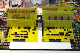
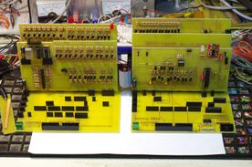
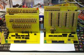
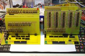
8080 CPU, built entirely by DTL-technology
September 09, 2017
Tragedy!
I have spent some time searching for reasons why certain parts don't want to cooperate and mostly it has been the classical fault.
For an example, reversed clock signals (180 degrees out of phase), some timing signals that was not entirely correct (signals to the memory control was 1/8 of the system clock was to late or to early), a glitch that occured at the end of each machine cycle that spooked the memory control, but only now and then.
The list goes on. But all those "problems" have been solved.
What I'm facing right now, however, is a fenomen I don't really understand. And that has to do with the REGISTERS.
Occasionally one bit of 16 is recognized as a ONE instead of a ZERO when I transfer data from other registers into the address latch (AL).
I'm using the AL as a buffer for 16 bit INC/DEC and this i a must for operating the PC and SP. For some reason PC seems to work fine, but SP doesn't. Or BC. Or HL.
This "glitch" is very rare, I might have to wait an hour or so before anything goes wrong.
I have some theories about this and the favourite one for now is that the inputs of the AL isn't happy with the signal levels from the register outputting the data.
That means I might have to rework all 16 REGISTER pcb. A prospect I'm not quite happy with.
--------------------------
Soo, at this stage I'm going to leave my DTL 8080 for a while.
I'm not abandoning this project, merely going to concentrate on something else, giving my rat-brain some time to process this AL problem.
A new project: Homebuilt 8080 Mk II (there is a link at the top.)
Back in 2013/2014 when all this started I had intention to use 74HC logic.
Now, with all knowledge I have gained from the DTL project I'm going to start up that old project again.
This DTL project will be collecting dust for now, until I find a solution the the AL trouble.
August 21, 2017
Finally some progress to report.
I now have added a simple protocol to my terminal program to send a text file over to the Microcode Loader.
That text file contains the microcode, which is stored in EEPROM. The first version of the microcode can be found here (txt file) and here (MS Excel).
So, that gives me a tool to in a relatively easy way modify the microcode and download it to the Microcode Loader when necessary. And it will be!
Downloading the microcode takes less than 2 minutes (after first having spent another 3 minutes extracting data from Excel).
Then, the actual loading of the stored microcode to SRAM at 8080 cold start takes no more than 2 seconds. Seems awfully fast though. There might be a bug somewhere..?
The earlier mishap with the slow Incrementer/Decrementer that would not be able to get the 8080 running at top speed (2 MHz) has now been compensated for
by adapting the microcode in such way that one extra T-cycle is used when nessercary to give the INC/DEC the extra needed time.
Besides the FETCH cycle, other instructions reading from or writing to memory have been adjusted sligthly to adress this and I can't see any loss of speed.
So, I'm back at 2 MHz again! For now...
Anyway, just because I can download new microcode at will doesn't mean that the Universe is on my side. Oh, no!
Now all weird thing is happening when the 8080 is starting up and that means I have some more bug hunting to do.
June 18, 2017
Progress is slower than I want it to be but it does go forward, one small step at a time.
I have now debugged the IO board.
This board expose the control signals to the outside world and also samples a few inputs like WAIT, INTERRUPT, BUSREQ and RESET.
It also exposes the DATA-bus.
All outputs are open collector, including the DATA-bus. It was simpler going with that than to build 3S-outputs. Each 3S-bit requires a lot of components and board space.
Open collector should work just as good. After all, the external bus will not be very fast so, all in all, it should be ok.
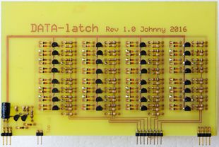
The IO board works together with an 8-bit WRITE-latch board and an 8-bit 3S buffer board.
I couldn't debug the IO board without debugging those bord as well, they are interconnected.
And of course I did find a small mishap with the WRITE-latch. I had crisscrossed two 8-pin connectors which ment I had to build a replacement. In the process I also found out
that I had missed a few timing signals.
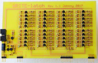
So, I built version 1.1 of the WRITE-latch, with an IDC connector of its side for those missing timing signals.
I also throw away the 8-bit 3S buffer board and added 8 2N2904 to the WRITE-latch as replacement.
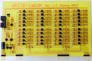
To make a long story a little bit shorter, I now have ended up with version 1.2 of the WRITE-latch. There was another little pesky signal that had to be involved which I, naturally, had forgotten. I made version 1.2 yesterday and hopefully that will be the end of it.
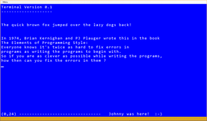
Another part I'm working on is a terminal program. Its written in C# and emulates a dumb 80x25 CRT.
Later on I will put in some higher functions from the old classic Wyse 50 terminal.
My 8080 will not have its own screen/keyboard but will instead talk over "RS232" to my PC. That is why I need a terminal program.
But that terminal program will also be used to download the source microcode from a spreadsheet to the MicroCode Loader, which in turn will store the microcode in an EEPROM.
Further, I have som ideas to use my PC as a hard drive for the 8080, using the RS232 connection to transfer program between the 8080 and my PC.
So, I have to build this terminal program myself to get all this functionality I want. Fun, fun, fun...
April 25, 2017
After living with this project for over 2 years, when the last PCB was finished I sat down and gasped for air, thinking that I might take a short break now, and continuing next week.
That was last september.
I have spent most of the time since then, watching cats & dogs on Youtube, so with that in mind you might be able figure out how much I needed that break.
However, I'm glad to inform you that I have started up the project again.
So, what I'm doing now? The answer is: hardware debugging!
I have spent some time the last 2-3 weeks to figure out why nothing seems to function properly...
Bug #1 - For some reason I had mixed up the RESET and /RESET lines, which meant everything was stuck at RESET when powered on.
Although a little annoying that was an easy fix.
Bug #2 - The PCB for the ALU Support had some missed solder points.
Bug #3 - The PCB for the Microcode Sequencer also had some missed solder points. Apparently this is a recurring feature. And a missing PCB trace.
More to it, I discovered while debugging the PCB that the fifth bit from time to time didn't want to toggle. Obviously a timing issue, but where?
I suspected the last D-FF because when I pressed down on the PCB with my finger where the last D-FF was, it did started to work. For a little while.
I could not make the D-FF faster so I had to slow down it's input signal. You might get a feeling of how the Sequencer is constructed by following this link.
All 5 D-FF is triggered in parallel and by some fluke when the 4:th one latched data from its 1-bit adder, the carry out from that adder had time to change value AND the sum out from the 5:th adder before the last D-FF had time to do its job.
The solution was to make the carry output from adder #4 slower, so I cut away a baker clamp from the last inverter (D44, bottom right transistor).
That gave me a whopping 10nS extra time and now D-FF #5 works great.
Bug #4 - A software one. I'm using an ATMega328P as a Microcode Loader to push out the microcode to the SRAM.
For now I'm just faking the microcode and substituting all 256 possible OpCodes with a NOP.
Also, every OpCode begins with 3 lines of FETCH code. Each OpCode has room for a total of 32 lines, minus 3 for the FETCH.
So I built a small assembler code with 3 loops - 256 OpCodes, 32 lines for each OpCode and 64 bit for each line.
And of course I made a beginner's mistake by letting loop #2 jump to high (line 340), which resulted in that ALL microcode sent to the SRAM consisted of the exact same 64 bit.
It took me the better time of a day to figure that one out, because I was convinced there was a hardware bug somewhere. Sigh.
This is the faulty code snippet
For those interested, here is a picture of the spread sheet I'm using to "program" the microcode.
And this is the correct one
After been washed, this is how it will look.
Line 445,446 and 447 is the FETCH and line 448 is a NOP instruction.
This is repeated for all 256 OpCodes.
After fixing all bugs, and doing some try and error with my assembler code, I finally succeeded to get the FETCH up and running !!
There is no memory connected to the CPU, that will be later, so for now the CPU fetches an instruction from thin air and is happy with that.
Here is a short video of the FETCH in action, just counting up the PC.
The left one is running at 1MHz and the one to the right a little bit slower.
When I shot this video there was some issues with the End Of Instruction PCB which ment that the Sequencer went through all 32 lines of microcode instead of just 4. So what you see here (the video to the left) is the CPU running at a speed of only 125KHz.
Lastly, I'm sorry to say that a string of 16 one bit full adders (7480) to INC/DEC the program counter (PC) isn't fast enough to run the CPU at 2MHz. It runs fine at 1MHz but not at 2.
It was a gamble I was aware of when I decided to skip the first version of the REGISTER (using 74283) and to rebuild it using slices.
However, because of the microcode approach I have choosen, there is a way to extend the time for the adders by inserting one extra line of microcode whenever an 16 bit add/sub has to be performed. That will cost, at 2MHz, an extra 500nS for each FETCH and also 500nS for some OpCodes such as PUSH/POP and a few others, but in general all other OpCodes will run as usual. But for now I will settle for 1MHz.
Sep 17, 2016
The CONTROL is finished !! I have no clue to it if it will work or not, but all PCB has been built. I'm most certain it will not work.
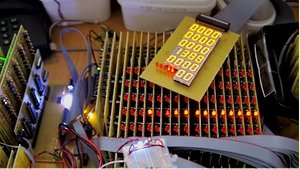
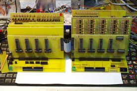
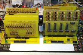
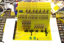
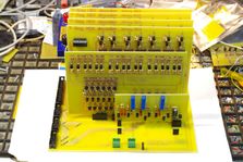
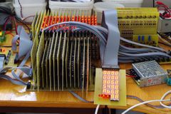
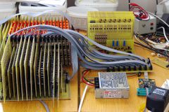
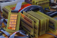
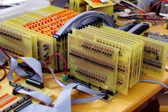
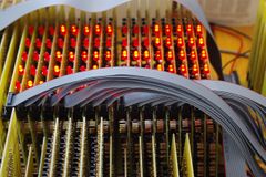
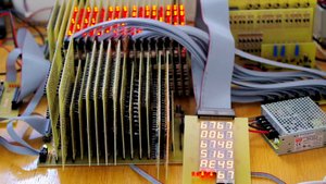
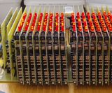
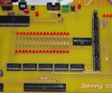
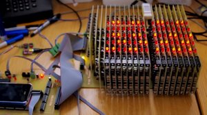
The CONTROL part is to the left. The top middle section is the REGISTER, the bottom middle is the ALU and the heap to the top right is the display MULTIPLEXER. The display multiplexer is no real part of the CPU, it's just for the fun of it.
What you see here is the complete 8080.
Total component count:
Resistors 3550
1N4148 1048
BAT42 4115
Transistors 2062
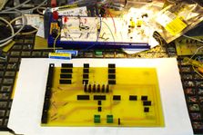
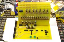
This below is the CONTROL being assembled. The left PCB is named/referred to as "Low side" and the one to the right as "High side".
Low/High side is something that has been stuck for a while. I have no recollection to why I named them like this, but it works for me, so...
July 16, 2016
The ALU is working!
I have spent the last 2 weekends testing all the functions of the ALU. Had to stomp on some bugs here and there to get it to work properly!
The usual stuff: a transistor mounted backwards, same with a diode, some solder points I had forgot.
I built the ALU last summer and did at that time some preliminary test of the basic functions (AND, OR, XOR, NOT, ADD).
However, I did not test the FLAGS, SUB(traction) with 2-Comp or 1-Comp and some other details.
To fully use everything in the ALU there has to be a correct sequence of control signals. There are a few of them... But the magnitude of testing all and everything by hand back then made me kind of losing interest for a while.
But that was then. Today I have a fully functional ALU and REGISTER.
Thanks to the "testdriver" (se below, June 18) having an AVR ATmega1284 (simulating the still missing CONTROL logic) and a few thousand lines of assembler code (no joke) I was able to run through every part of the ALU. And as a small bonus I have much of the needed microcode in those assembler lines as well.
My focus now will be more or less 100% on the CONTROL circuitry. There are a few tiny questionable bits of the microcode layout to fix. Once that is done its time to make some more PCBs.
July 3, 2016
Today I attached the ALU to the Test Driver. I have not touched the ALU for almost a year. Time just flies by.
The plan is to let the Test Driver simulate the CONTROL and to see what ALU signal lines has to be yanked, and in what order, to get expected result. It will be a much-needed freshen up of what a year ago was absolutely (mostly) crystal clear.
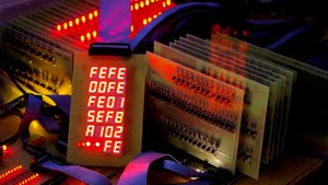
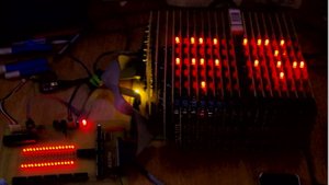
Also, not related to the 8080 function whatsoever, I have built a MULTIPLEXER that displays the register contents, Flags and Accumulator, in HEX-format (5 LED's for the Flags).
That has been in the plans from the beginning and finally I have it up and running. To be honest, when the CPU is up and running (at speed, I hope) there will be no chance to actually read from the display whats going on, it will just be a blur resembling some 8888. Nevertheless, the awe factor makes it worth the while.
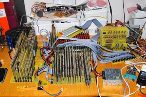
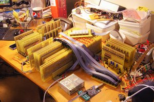
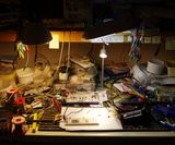
Here is some pictures of the "well planned" layout of what I have so far...
Showing of the MULTIPLEXER :
(MP4 videos, 1.43 MB and 4.7 MB)
If it doesn't play in your browser, download the file to your hard drive and play it from there.
I counted the number of components for the ALU and this is what I came up with..:
June 18, 2016
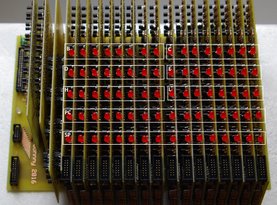
The REGISTERS are finished, and is working as expected! That is, after some debugging. Found a few solder point I had missed but thats all. Phew !
It weighs 1.4 kg and consumes approx 1.5 A at 5 V.
Other facts:
Resistors | 1828 |
Capacitors | 36 |
1N4148 | 248 |
BAT42 | 2056 |
Transistors | 1058 |
Total number of holes to drill for those | 11510 |
It took 11 hours to drill all 16 slices, using this:
The MUX and 3S cards not included in those 11 hours. Or the base board.
Running test :
(MP4 videos, 4.8 and 3.0 MB)
If they doesn't play in your browser, download the file to your hard drive and play it from there.
All bits are organized as in the picture to the left (click on it). There is also a WZ register and a address latch - AL.
AL is 16 bit wide, all other are 8 bit. AL can only be written to from BC, DE, HL and WZ and of course the reverse of that, AL can be read and written into BC, DE, HL and WZ. Not all of those combinations is used by the 8080 but the functionality is there.
In the video above (the one to the right) I'm running a short program on the "testdriver" that by use of a bunch of 74HC595, controlled by a ATmega1284P, yanks the control lines, as the yet to be completed CONTROL unit will do later on, when its finished.
The controller increments an internal register and then write that info into the C register. It also write it to the B register.
After that it read back the value from C and writes it into H. The L is written by the 1 complement of H.
All this is a test to see if everything cooperates.
The PC is incremented this way : First the both MUX'es are disabled. PC (PChigh and PClow) is opened for reading and the AL is primed for writing. There is a clock pulse, called Phi2, that on its back edge locks data from PC into AL. At the same time the Incementer/Decrementer is told to do increment of AL. Then the Incrementer/Decrementer is opened for reading and PC is primed for writing. Phi2 is applied and there you have it.
The SP works the same way except here I'm telling the Incrementer/Decrementer to decrement instead.
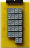
The IDC connector you see on each "slice" board is going to be used to extract information from BC, DE, HL, PC and SP by a "multiplexer" that will collect data and by use of some 7-segment HEX decoders display the register contents onto the display to the right:
May 29, 2016
Made 2 more pcb's for the REGISTERS : another MUX aka 74LS245, and another 8 bit 3S buffers.
Now there are "only" 15 more register slices missing. Blank pcb's has been ordered and they will, hopefully, be delivered at the end of the next week.
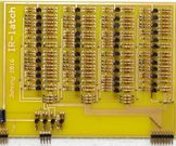
I have also built the IR Latch pcb.
May 22, 2016
Added new pages for REGISTER and CONTROL.
Have started a new adventure - building the CPU registers. Actually, I did that last year but I was never satisfied with what I came up with. It did not "taste" quite right.
A new solution was needed and the SLICE was born (very early this spring).
This weekend I have been verifying the prototype and, of course, found a couple of bug's in the process. One of them was a simple one, two lines crossing each other effectively making a short. The other one was (is) more complicated. From the beginning I have been using the transistor SS9018 for "speed" and BC547A for everything else, like in the old CPU REGISTER part. For slow speed thats was all well, and they are fairly compatible at logic levels.
Introducing my new favourite KSP10 for the high speed parts (CONTROL) has worked out quite well so far, but now when I'm starting to interface KSP10 and SS9018 against each other I noticed that they don't play well together.
Despite the fact I like KSP10 for, well, everything, the harsh reality is that the ALU is all made out of SS9018 !! More of this in the BUG section.
At another note: I have made 4 pcs of 7-seg HEX Decoder. All from the beginning i have had plans to display the contents of all of the CPU registers, either by a bunch of LED's or by a bunch of 7-seg displays. For that I had to pull out 96 bit's of information from REGISTERS and ALU and frankly, that isn't so hard. Just a bundle of wires.
But, for some reason, I tend to overdo things. Introducing multiplexing!
Outside of the 8080 there will be another large board with multiplexing timers, counters, 7-seg decoders/drivers and so on.
For all that to happen there has to be multiplexing logic on all the REGISTER boards as well. (The ALU has that in place, already.)
If you ever wonder what the 14-pin IDC connector has to do on the REGISTER SLICE (upper right), that's part of the multiplexing design.
April 30, 2016
I've had some personal problems that did put a damper on virtually everything this winter/spring.
Understandably I haven't done much with my 8080 project.
But, I'm back, feeling better!
Despite everything, I have managed to do some work now and then and I can now report that I have completed the schematic for the CONTROL logic.
I have made some compromises, simplifying the CONTROL logic at the expense of overall performance. But I can live with that.
Now, almost 8 month of silence doesn't mean there have not been things done :
- Interrupt is back!
- Made a new "friend"... KSP10 is now my transistor of choice! The old SS9018 is out. Take a look at this page to see why. KSP10 at the bottom
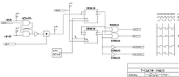
- T-Cycle Generator is built and working comfortably at 8 MHz.
- Microcode Loader is built. This board also house the RESET logic. The 28 pin chip is a Atmega328P and it's only job is load the microcode into the SRAM. Nothing more.
- Microcode SRAM (2 boards) is built.
- Microcode Sequencer is built.
- Started (on paper) to integrate CONTROL, ALU, REGISTER and I have, naturally, found some bugs.
I will follow up with more details later (not another 8 month later, promise).
Sep 6, 2015
Defeat (for now)! I find it difficult to make a transistorized JK FF to work properly at speeds up to 8 MHz. I mean, they do work, but not as good I want them to.
Therefore I will surrender to the fact that for the time being I'm having to rely on some 74HC/AC circuits for the T-cycle generator.
Anyway, the T-cycle circuit is being placed on it's own circuit board and if I later on ever find a solution to my JK FF trouble there is no more to that than just swap out the old circuit board for a new one.
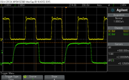
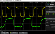
I made a version #2 of the "high speed" JK FF from aug 23, 2015 (below). It will be the work horse for other places in the control logic, not needing so much speed, like the microcode sequencer. The sequencer only see 2 MHz as it inputs and that should not be a problem. Picture below shows the JK toggle at 2 MHz and at 5 MHz.
I'm not (!) going to show a picture of it toggling at 10 MHz. It would just hurts your eyes.
Edge triggered JK FF Version #2
Sep 2, 2015
I have decided to "hide" most of the control logic in a 64 bit wide parallel microcode (I started out with 40 to 48 bit) hopefully giving me a chance to possibly finish this project.
Also, I have started to put together all odd circuits that's needed to make the control logic. At this point all there is, is a bunch of sketches here and there and some vague ideas in my head.
I'm also trying to put in a single step mechanism. And why not?
And, at this point the interrupt logic has to go. It seems to be a little too complicated to implement it as I wanted it to, but I will try to keep the option open for a later addition.
The control logic will be splitted on to two parallel pcb's, one for the REGISTER and another one for the ALU.
Aug 23, 2015
Work! A very disturbing moment in my everyday life!
My employer expect great deeds out of me, like squeeze water from a piece of granite with only my bare hands. This means that I can not dedicate so much time on my little project that I would like. Nevertheless, I have finally succeeded with a small milestone today: A working edge triggered JK flip-flop that toggles at 10 MHz.
There is still some tweeking to do but all things considered I'm happy.
I have tried out several variants of edge triggered JK FF, including 74LS73, but they only work, reasonable, well in LTspice. In real life not so well. Not at all, actually!
After I have done the tweeking I'm going to make two more of this one plus some NOR-gates and se how they work together, as my final prototype of the T-cycle generator. I would hate myself if I have to go for plan B and use some IC, but, as the only part that require high speed I might be able to live with such compromise.
Aug 12, 2015
The ALU has been put together, and some parts of the REGISTERS cards. Yet to be tested. The ALU weigh in at 1.4 Kg!
My "test driver" has been completed as well. Again, yet to be tested.
More photos in the gallery section.
Currently I'm working on the T-cycle circuit and the microcode sequencer. My currect gate solution doesn't work at those speed I want them to, so I had to improve them by going back to basic TTL 7400 logic, but instead of using a transistor for the logic I'm using a diode, so there is still a DTL gate at play. I have breadborded one of thoose (7404) and it works beautifully at 10 MHz.
Next on the schedule is to make a card with 2 JK Flip-Flop (T-cycle circuit) and see how it turns ut. 8 MHz is my goal for a 500 nS T-cycle.
Aug 5, 2015
This "Page" is published to the net. At this point there isn't much to see, I hope to find some time shortly to fill it with little more info.
I have built the ALU, yet to be fully tested. The ALU seems to do what it should but I have not had the opportunity to test the FLAG-register and the DAA.
The ALU "motherboard", rev 2.4 has been drilled but nothing more. I have to finish that before I can hook it up the my new, yet to make, test board.
I have made enough circuit boards for the register part so that can be tested as well : BC, DE, HL, PC, SP and WZ. But only the PC is actually made at this point, And the address latch, the address 3S-buffers and a version of 74245 to isolate the register from the internal D-bus. Plus 2 7483 to be used as address incrementer/decrementer.
Also in the pipeline, there is a test circuit to be built and some PC-program to be written to run this test circuit.
I hope to able to make that circuit board over the weekend.
This test circuit have a ATmega1284P and will be hooked up to the ALU and Registers boards, emulating the timing circuit, instruction decoder and everything else.
I hope.
Pre Aug 5, 2015
Over a year with design, try and error, and finally actually making some circuit boards.
I will not go into all details of the past.
Homebuilt CPUs WebRing
Join the ring?
To join the Homebuilt CPUs ring, drop Warren a line, mentioning your page's URL. He'll then add it to the list.
You will need to copy this code fragment into your page (or reference it.)
Note: The ring is chartered for projects that include a home-built CPU. It can emulate a commercial part, that′s OK.
But actually using that commercial CPU doesn′t rate. Likewise, the project must have been at least partially built: pure paper designs don′t rate either.
It can be built using any technology you like, from relays to FPGAs.
